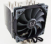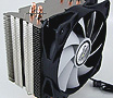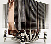
TOP 5 Heat Sinks TOP 5 Low Profile Heat Sinks TOP 5 Liquid Coolers
Heatsinks by Brand / Mfgr Reviews + Articless Advanced Search
|
TOP 5 Heat Sinks TOP 5 Low Profile Heat Sinks TOP 5 Liquid Coolers Heatsinks by Brand / Mfgr Reviews + Articless Advanced Search |
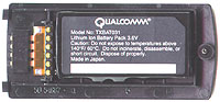
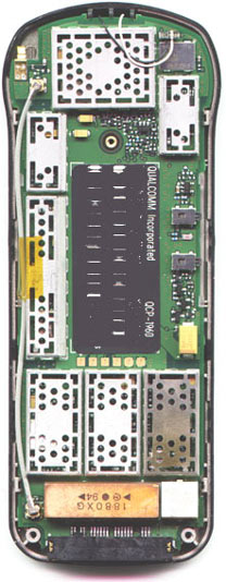
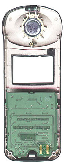
Inside the Cell Phone Cell phones are everywhere. Look to any corner of the street, office or home and chances are you will see at least one of them. While prices for cellphones have been dropping like a rock, new models are always more expensive than one's just a few months old and offer services like email, and internet access. But have you ever wondered what's inside these ever-shrinking devices? Since we are fairly inquisitive around here, we cracked open a phone to see what was inside. Luckily there are even heatsinks in a cellphone, so there is at least one thing we can discuss. Antenna's were never my strong point :) Let the dissection begin!
|
|
|||||||||||||||||||||||||||||||||||
|
Find a Heatsink . Latest Heatsink Reviews . Top 5 Heatsinks Tested . Top 5 Low Profile Heatsinks . Top 5 Liquid Coolers . Heatsinks by Mfgr / Brand |
Social Media |
FrostyTech.com Info . Feedback . Contact Us / Heatsink Submissions . Submit News . Privacy Policy |
 | |
© Copyright 1999-2025 www.frostytech.com All Rights Reserved. Privacy policy and Terms of Use Images © FrostyTech.com and may not be reproduced without express written permission. Current students and faculty of accredited Universities may use Frostytech images in research papers and thesis, provided each image is attributed. | ||||